
Quantum Reality
Shubhayan Mukherjee (木和班)
Research Scholar (Ph.D. Candidate)
NEXT-G for materials design

Latest
-
Award of Excellence in Materials Science from the National Synchrotron Radiation Research Center in 31st NSRRC Users’ Meeting & Workshops, Taiwan (September 2025).
-
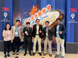
TMS 2025 Student Travel Grant Award by Functional Materials Division (FMD) in American Minerals, Metals and Materials Society (154th TMS Annual Meeting & Exhibition).
Research
My work during my visit in NIMS (Japan) explores how combining Ar-FAB oxide removal with E-VUV irradiation enables a new surface modification pathway in galvanic replacement.
Lowering interfacial free energy reduces the nucleation barrier (ΔG*) and stabilizes the coupled Cu dissolution–Ag⁺ reduction reactions. This leads to continuous, uniform Ag growth while suppressing dendritic structures - offering a new physics perspective for controlled thin-film deposition.
Mukherjee, S., Shigetou, A., Chou, Y.-H. & Lin, S.-K. Modified galvanic replacement using ethanol vapor-assisted vacuum ultraviolet (E-VUV) for enhanced Ag deposition. Mater. Lett. 374, 139482 (2025). https://doi.org/10.1016/j.matlet.2025.139482
Disciplines
Experimental Materials Physics | Crystallography | Intermetallic Compound (IMC) | Electromigration | Electroplasticity | Phase Stability | Synchrotron Radiation | Surface Modification
Skills
Scanning Electron Microscopy (SEM) | Electron Back Scattered Diffraction (EBSD) | Energy Dispersive Spectroscopy (EDS) | X-Ray Diffraction (XRD) | Transmission Electron Microscopy (TEM) | ARC melting furnace | Nanoindentation | Laue White Light Nanodiffraction | Synchrotron Radiation (TLS & TPS, NSRRC, Taiwan) | X-ray photoelectron spectroscopy (XPS) | Ar Fast atom bombardment (FAB) Irradiation | Vacuum Ultraviolet (VUV) Surface Treatment | Raman Spectroscopy

 |  |  |  |  |  |  |
|---|---|---|---|---|---|---|
 |  |  |  |